Friday, April 19, 2024

Canon releases LI5030 sensor


Canon’s 2.8 MP LI7060 CMOS sensor is equipped with an HDR drive function that achieves a wide 120 dB range at low noise levels. This wide range results in a greater ability to extract usable information even where there is a substantial difference between the lightest and darkest areas of an image. Even when using the sensor during normal drive operation, the sensor can achieve a dynamic range of 75 dB.


The LI5040 and 3U5MGXSBA global shutter image sensor employs an advanced pixel design introducing drive readout and gathering structures which help significantly reduce noise, and contributing to a wide dynamic range with a power consumption of 500mW. Equipped with a 3.4μm pixel size and all pixel progressive reading at 120fps, the 2/3” sensor size with 5.33 million effective pixels (2592 x 2056) easily allows for applications in machine vision and other industrial environments where smaller size and high performance are required. It is available in RGB, Monochrome, and a specialized RGB‐NIR color filter.


LI5030SA is a CMOS type of solid-state image sensor with a 35mm full frame effective pixel array of 19 Megapixels. It uses a global shutter function instead of a conventional rolling shutter. It enables simultaneous exposure timing for all 19 megapixels. It can output an effective 5688 x 3334 pixels of video at 57.99 fps and 12bit via 24 channels of digital signal output. LI5030SA series consists of LI5030SAC (color), LI5030SAI (RGBIR), LI5030SAM (monochrome), and LI5030SAN (Naked). LI5030SAN does not have a microlens or color filter.
The high sensitivity, resolution, and global shutter of this sensor along with multiple color filter variations makes the LI5030 a great choice for a wide array of applications such as microscopes, factory automation, traffic surveillance, drone vision, etc.

Wednesday, April 17, 2024

Sony IMX900 videos


This video presents Sony's 1/3.1" global shutter image sensor IMX900 with approx. 3.2 effective megapixels that is compact, high-resolution, and has improved near-infrared sensitivity. Here are its three features.
=================================
Chapters
 =================================
0:00 Opening
0:40 Compact, high resolution(1/3.1" 3.2MP)
1:12 Improved incident light angle dependency
3:00 Enhanced NIR region sensitivity
3:41 Ending
------------------------------------------------------------


This video presents Sony's IMX900 global shutter image sensor, which is ideal for industrial applications such as barcode reading, picking robot, and AMR (autonomous mobile robots). 
Here are the three functions that support optimal imaging for different scenarios.
=================================
Chapters
 =================================
0:00 Opening
0:27 Fast Auto Exposure
1:42 Quad HDR(High Dynamic Range)
2:22 Quad Shutter Control

Monday, April 15, 2024

EgisTec to acquire Curious

Taiwan-based IC design house Egis Technology (EgisTec) has announced plans to acquire Curious, a Japan-based IP and fabless chipmaker, in a share swap transaction valued at NT$525 million (US$16.4 million). 

Link: https://www.digitimes.com/news/a20240402PD213/egistec-inpsytech-ip-licensing-mergers-and-acquisitions.html

Curious designs IP for image sensors:
http://www.curious-jp.com/en/

Egis makes fingerprint sensors including under-display optical sensors, including those used in older Samsung Galaxy S9 and S9+ phones:
https://www.egistec.com/en/


Sunday, April 14, 2024

Job Postings - Week of 14 April 2024

Samsara

Lead Camera Systems Engineer

San Francisco,, California, USA

Link

Fraunhofer HHI Telecommunications

Scientist Photonic for single photon detectors

Berlin, Germany

Link

Fraunhofer HHI Telecommunications

Scientist photonic Foundry Platform

Berlin, Germany

Link

RTX Raytheon

Principal Signal and Sensor Modeling Engineer

Tucson, Arizona, USA

Link

Swansea University

Funded EPSRC DTP PhD Scholarship: Diamond NV Quantum Sensor

Swansea, Wales, UK

Link

Apple

Optical Characterization and Simulation Engineer

Cupertino, California, USA

Link

TU Delft

Phd Position for Low-power Broad-spectrum Image Sensor with Local Smart Data Processing

Delft, Netherlands

Link

Thermo Fisher Scientific

Engineer III, Systems Design

Hillsboro, Oregon, USA

Link

Weizmann Institute

Tracking in SF-QED experiments and R&D of wide-bandgap detectors

Rehovot, Israel

Link

Saturday, April 13, 2024

X-FAB annonces BSI process for next gen image sensors

Link: https://www.xfab.com/news/details/article/x-fab-enhances-image-sensor-performance-through-back-side-illumination

X-FAB Enhances Image Sensor Performance Through Back-Side Illumination

NEWS – Tessenderlo, Belgium – Apr 03, 2024

Presenting a foundry route to medical, automotive and industrial customers that combines boosted sensitivity, larger pixel size and more extensive sensor area

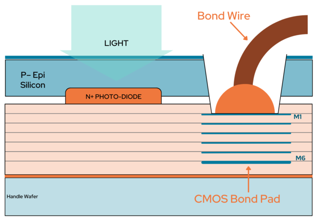
X-FAB Silicon Foundries SE, the leading analog/mixed-signal and specialty foundry, has just announced a major addition to its optical sensor offering. Aimed at use in next generation image sensor fabrication, the company is now able to provide a back-side illumination (BSI) capability in relation to its popular XS018 180nm CMOS semiconductor process.

Through BSI, imaging devices’ performance characteristics can be significantly enhanced. It means that the back-end process metal layers do not block the incident light from reaching the pixels, increasing fill factors by up to 100%. This is highly beneficial in situations of low-level illumination – as higher pixel light sensitivity can be achieved. BSI also offers the added advantage of significantly reducing the crosstalk between neighboring pixels, due to shorter light paths, leading to better image quality. Though small-pixel BSI solutions for 300mm wafers with high-volume consumer usage are commonplace, there are very few options available for image sensors with stitched large-pixel arrangements for 200mm wafers, especially when additional customizations are required. The new X-FAB BSI capability brings new possibilities, allowing customers with even the most demanding application expectations to be served - such as those involved in X-Ray diagnostic equipment, industrial automation systems, astronomical research, robotic navigation, vehicle front cameras, etc.

Leveraging the XS018 platform, which offers high readout speeds and exhibits low dark currents, image sensors with multiple epi options will be produced. An ARC layer can be added and then tuned in accordance with particular customer requirements. The accompanying X-FAB support package covers a full workflow from initial design through to the shipment of engineering samples, with a comprehensive PDK included.

“BSI technology has become increasingly prevalent in modern imaging devices, thanks to its ability to boost image quality by placing light-sensitive elements closer to the light source and avoiding unwanted circuitry obstructions. This is proving very useful in environments where light is limited,” states Heming Wei, Technical Marketing Manager for Optical Sensors at X-FAB. “Though much of this uptake has been within the consumer electronics sector, there are now numerous opportunities emerging in the industrial, automotive and medical markets. Via access to X-FAB’s BSI foundry solution, it will now be possible for these to be properly attended to, with a compelling offering being provided that brings together heightened sensitivity, enlarged image sensor dimensions and bigger pixel capacities too.”


Monday, April 08, 2024

Sony news and videos

From https://www.sony-semicon.com/en/news/2024/2024032801.html

New Fab Expansion at Sony Device Technology (Thailand) Co., Ltd.

Atsugi, Japan — Sony Semiconductor Solutions Corporation today announced that, starting in February 2024, it has begun the operations with several production lines at the new fab built on the premises of Sony Device Technology (Thailand) Co., Ltd. (“SDT”), a production center responsible for assembly processes of semiconductors. The opening ceremony was held today, officiated by top executives from Sony Semiconductor Solutions Group led by Terushi Shimizu, President and CEO of Sony Semiconductor Solutions and Yoshihiro Yamaguchi, President of Sony Semiconductor Manufacturing, SDT Managing Director Takeshi Matsuda. It was witnessed by guests including Japan’s Ambassador to Thailand, Mr. Masato Otaka, Mr. Wirat Tatsaringkansakul, BOI Deputy Secretary General and other VIPs. 

SDT serves as a production center for the assembly of the main product line within Sony’s Imaging & Sensing Solutions business. The new fab, dubbed “Building 4,” will be utilized for the assembly of image sensors for automotive applications and display devices as well as the mass production of laser diodes for data center application.

Going forward, SDT plans to expand production facilities at Building 4 in line with market trends, while also planning to create approximately 2,000 new jobs with this new operation, thereby contributing to local employment and expanding the semiconductor industry in Thailand.

In addition, SDT has been operating its facilities on 100% renewable energy since fiscal year 2021. In the clean room of Building 4, the air conditioning system controls cleanliness, temperature and humidity by focusing on areas of need, and recycling technology for waste heat and hot water has also been adopted. Furthermore, SDT plans to cover the roof area of Building 4 with solar panels, with operations scheduled by the end of 2024 (calendar year). By accelerating the initiatives to reduce energy consumption and adoption of renewable energy, SDT will continue to run on 100% renewable energy even after Building 4 goes into full operation.

“With the completion of Building 4, we are very pleased to be able to deliver to more customers, a product line-up whose market is expected to expand over the medium to long term,” said Takeshi Matsuda, Managing Director of Sony Device Technology (Thailand) Co., Ltd. “As an overseas manufacturing site of Sony Semiconductor Solutions Group, SDT will contribute to the sustainable evolution of Sony’s business as well as society.”

-----------------------------

Two new videos about IMX900 sensor on YouTube:


This video presents Sony's 1/3.1" global shutter image sensor IMX900 with approx. 3.2 effective megapixels that is compact, high-resolution, and has improved near-infrared sensitivity. Here are its three features.


This video presents Sony's IMX900 global shutter image sensor, which is ideal for industrial applications such as barcode reading, picking robot, and AMR (autonomous mobile robots).  Here are the three functions that support optimal imaging for different scenarios.

Sunday, April 07, 2024

Job Postings - Week of 7 April 2024

California Institute of Technology  SRL

Instrument Scientist

Pasadena, California, USA

Link

ERC Centre de Nanosciences et de Nanotechnologies

PhD position :Integrated electro optical modulators and photodetectors in the mid-IR spectral range.

Palaiseau, France

Link

Omnivision

Product Marketing Manager

Santa Clara, California, USA

Link

University of Edinburgh

Research Associate in Short Wave Infrared LIDAR Sensors

Edinburgh, Scotland, UK

Link

United Imaging America

Laparoscope Image Signal Processing Expert

Houston, Texas, USA

Link

ETH Zurich

DMAPS Detector Development (DRD3 Collaboration)

Zurich, Switzerland

Link

Leonardo DRS

Principal Electro-Optical Engineer

San Diego, California, USA

Link

NASA Goddard SFC

Far-Infrared Detectors for Space-Based Low-Background Astronomy

Greenbelt, Maryland, USA

Link

KLA

Senior / Staff Electrical R&D Engineer (Hardware)

Singapore

Link

Saturday, April 06, 2024

STMicroelectronics has an opening in Paris

 STMicroelectronics

Expert in image processing algorithms for optical sensors (or)            Paris, France      Link
Expert en algorithmes de traitement d'image pour capteurs optiques    


Thursday, April 04, 2024

Available: a Ph.D. Scholarship under Prof. Guy Meynants

KU Leuven

PhD on temporal noise reduction in CMOS image sensors     Geel, Belgium     Link