Canon publishes promotional videos of its 120MXS 120MP 2.2um pixel APS-H sensor and 35MMFHDXS 1080p 19um pixel full-frame sensor:
Saturday, March 31, 2018
Yole on CIS Wafer Starts
Yole Developpement report "Wafer Starts for More Than Moore Applications" shows that CIS consumes more wafers than RF devices and MEMS, but less than power management devices:
"We expect 12-inch wafer demand to grow from 3.3 million units in 2017 to 7.5 million in 2023, mainly fueled by Backside Illumination CMOS Image Sensors (BSI CIS) (3D stacked BSI, 3D hybrid BSI)."

"We expect 12-inch wafer demand to grow from 3.3 million units in 2017 to 7.5 million in 2023, mainly fueled by Backside Illumination CMOS Image Sensors (BSI CIS) (3D stacked BSI, 3D hybrid BSI)."

Friday, March 30, 2018
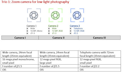
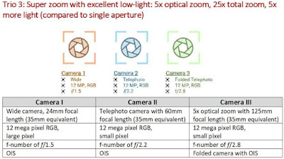
Corephotonics on Triple Cameras
EETimes publishes Corephotonics article "Triple Cameras: Are Three Better Than Two?" by Gil Abraham. Few quotes:
"In this article, we will discuss some motivations for adding a third camera to the smartphone imaging complex, the challenges it brings and some possible solutions.
...This first phase of dual cameras continued until mid-2016, while various OEMs were testing dual camera technologies in some of their flagship smartphones, using different dual camera setups, including depth-only, RGB-Mono and Wide-and-Wider duos. There was still no "killer camera app" identified, nor a winning dual camera configuration.
...Apple managed to shine the spotlight on a specific dual camera configuration, Wide+Tele, as the premium camera setup.
...the addition of that third camera carries significant challenges (and rewards), while opening up a wide array of possibilities and configurations for smartphone manufacturers.
Challenge 1: “Real-estate” & Cost
The added cost of the third camera directly depends on the camera configuration, as explained later in this article, and could be anywhere between $10 to $30.
Challenge 2: Calibration
In case all three cameras need to be perfectly calibrated one with respect to the others, the camera assembly process must be carefully designed, and the expected yield would be lower. In turn, these have direct effect on the total camera cost."


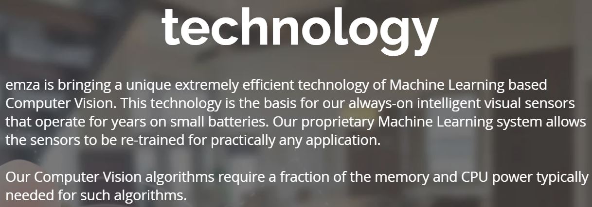
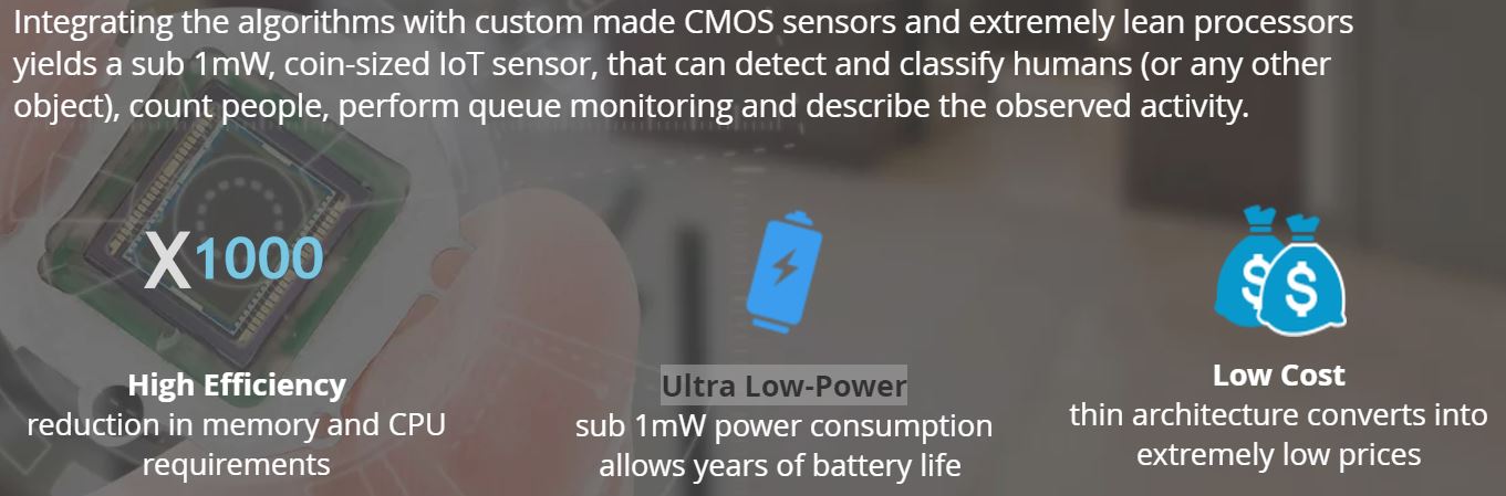
Himax Acquires Emza Visual Sense
GlobeNewswire: Himax has decided to exercise its options to fully acquire Emza Visual Sense Ltd. Terms of the investment were not disclosed. The transaction is expected to close by the end of the second quarter, 2018.
Emza is an Israeli company dedicated to the development of extremely efficient visual sensors that include proprietary machine-vision algorithms and architectures that enable always-on visual sensing capabilities, achieving orders of magnitude improvement in power consumption, price and form factor. Aiming at the booming computer vision market, Himax made a strategic cash investment for 45.1% equity of Emza in April 2017, with one-year options to acquire the remaining 54.9% of Emza’s equity and all outstanding stock options. Emza will continue as it is after the acquisition, and will maintain Emza company brand as well as the WiseEye brand product lines.
“With the full acquisition of Emza, Himax will be uniquely positioned for IoT solutions, which require tight integration of the critical skills and knowledge of Himax’s CMOS technology and ASIC design with Emza’s computer vision algorithms. Himax will be positioned to offer significant value to our customers and to enter new markets beyond consumer electronics, such as connected homes, smart buildings and security, and extend our reach into new IoT markets with interest in other Himax products such as our 3D sensing solutions,” said Jordan Wu, CEO of Himax.
“Our team members are excited about becoming part of the Himax family. The synergy between the two companies and our mutual skills will accelerate the development of highly integrated turn-key IoT solutions to take machine learning-based computer vision applications to a whole new level of performance, price and autonomy. We will continue to pursue the IoT market and customers,” said Yoram Zylberberg, CEO of Emza.
Thursday, March 29, 2018
Reuters: Uber Cars Emphasize Radars over Imaging
Reuters publishes an article on Uber self-driving Volvo XC90 sensing module comparing it with Ford Fusion autonomous cars that Uber used in its older fleet. One can see that the latest Uber-Volvo cars rely more on radars and less on cameras and LiDARs:
"Autonomous vehicles operated by rivals Waymo, Alphabet Inc’s self-driving vehicle unit, have six lidar sensors, while General Motors Co’s vehicle contains five, according to information from the companies.
The safety of Uber’s self-driving car program is under intense scrutiny since Elaine Herzberg, 49, was killed last week after an Uber Volvo XC90 SUV operating in autonomous mode struck and killed her while she was jaywalking with her bicycle in Tempe, Arizona."

RTN and Photon Shot Noise Reduction in Multi-Aperture Cameras
MDPI Sensors journal publishes a paper "Multi-Aperture-Based Probabilistic Noise Reduction of Random Telegraph Signal Noise and Photon Shot Noise in Semi-Photon-Counting Complementary-Metal-Oxide-Semiconductor Image Sensor" by Haruki Ishida, Keiichiro Kagawa, Takashi Komuro, Bo Zhang, Min-Woong Seo, Taishi Takasawa, Keita Yasutomi, and Shoji Kawahito from Shizuoka and Saitama Universities
"A probabilistic method to remove the random telegraph signal (RTS) noise and to increase the signal level is proposed, and was verified by simulation based on measured real sensor noise. Although semi-photon-counting-level (SPCL) ultra-low noise complementary-metal-oxide-semiconductor (CMOS) image sensors (CISs) with high conversion gain pixels have emerged, they still suffer from huge RTS noise, which is inherent to the CISs. The proposed method utilizes a multi-aperture (MA) camera that is composed of multiple sets of an SPCL CIS and a moderately fast and compact imaging lens to emulate a very fast single lens. Due to the redundancy of the MA camera, the RTS noise is removed by the maximum likelihood estimation where noise characteristics are modeled by the probability density distribution. In the proposed method, the photon shot noise is also relatively reduced because of the averaging effect, where the pixel values of all the multiple apertures are considered. An extremely low-light condition that the maximum number of electrons per aperture was the only 2 e− was simulated. PSNRs of a test image for simple averaging, selective averaging (our previous method), and the proposed method were 11.92 dB, 11.61 dB, and 13.14 dB, respectively. The selective averaging, which can remove RTS noise, was worse than the simple averaging because it ignores the pixels with RTS noise and photon shot noise was less improved. The simulation results showed that the proposed method provided the best noise reduction performance."


"A probabilistic method to remove the random telegraph signal (RTS) noise and to increase the signal level is proposed, and was verified by simulation based on measured real sensor noise. Although semi-photon-counting-level (SPCL) ultra-low noise complementary-metal-oxide-semiconductor (CMOS) image sensors (CISs) with high conversion gain pixels have emerged, they still suffer from huge RTS noise, which is inherent to the CISs. The proposed method utilizes a multi-aperture (MA) camera that is composed of multiple sets of an SPCL CIS and a moderately fast and compact imaging lens to emulate a very fast single lens. Due to the redundancy of the MA camera, the RTS noise is removed by the maximum likelihood estimation where noise characteristics are modeled by the probability density distribution. In the proposed method, the photon shot noise is also relatively reduced because of the averaging effect, where the pixel values of all the multiple apertures are considered. An extremely low-light condition that the maximum number of electrons per aperture was the only 2 e− was simulated. PSNRs of a test image for simple averaging, selective averaging (our previous method), and the proposed method were 11.92 dB, 11.61 dB, and 13.14 dB, respectively. The selective averaging, which can remove RTS noise, was worse than the simple averaging because it ignores the pixels with RTS noise and photon shot noise was less improved. The simulation results showed that the proposed method provided the best noise reduction performance."


Wednesday, March 28, 2018
Powerchip Files IR-Enhanced Pixel Patent Application
Powerchip files US20180040651 patent application "Image sensor and related fabrication method" by Shih-ping Lee, Yu-an Chen, Hsiu-wen Huang, and Chuan-hua Chang.


Ambarella Announces 2nd Gen CV Processor
BusinessWire: Ambarella introduces the CV2 camera SoC combining advanced computer vision, image processing, 4Kp60 video encoding, and stereovision in a single chip. CV2 targets advanced automotive, IP security, drone, and robotic applications, delivering up to 20 times the deep neural network performance of Ambarella’s first generation CV1 chip. Fabricated in 10nm process, CV2 offers extremely low power consumption.
“With CV2 we have dramatically increased our computer vision performance and combined it with full SoC functionality,” said Fermi Wang, CEO of Ambarella. “As the highest performance member of our new CVflow family, CV2 delivers both the deep neural network and stereovision processing required for the most advanced automotive and security cameras.”
CV2 Computer Vision SoC Features:
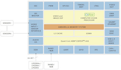
- CVflow processor with CNN/deep learning support
- 4Kp60/8MP AVC and HEVC encoding with multi-stream support
- Multi-sensor support for 3-channel electronic mirror and 4-channel AVM systems, multi-channel stereo sensing systems (up to 4 stereo pairs), and multi-imager IP cameras
- Quad-core 1.2-GHz ARM Cortex A53 with NEON DSP extensions and FPU
- Real-time hardware-accelerated 360-degree de-warping and Lens Distortion Correction (LDC) engine
- Multi-channel ISP with up to 800 MP/s input pixel rate
- Multi-exposure HDR and WDR processing
- LED flicker mitigation
Cepton Unveils Vista LiDAR
BusinessWire: Cepton Technologies unveils its Vista LiDAR sensor, said to deliver the best-in-class performance to the automotive market when compared to current LiDAR technologies. The 120-line-equivalent scanner delivers 200 meters of range and 0.2 degrees of spatial resolution. The Vista LiDAR is significantly smaller than most solutions on the market and uses fewer than 10 watts of power.
The Vista sensor is the fourth LiDAR product developed by the fast paced Cepton team over its first 20 months in operation. Built on Cepton’s patented micro-motion technology (MMT) platform, Vista has no rotational or frictional parts, consisting only of high maturity automotive components for expedited automotive grade certification. Vista LiDAR samples are available today for Cepton’s automotive partners to evaluate in their self-driving fleets. Automated volume production will start in Q2, 2018.
“Performance is very important for our automotive customers, but when it comes to scale deployment, everything matters. Vista provides an unmatched combination of small size, low power, long range and high resolution,” says Mark McCord, VP of engineering and co-founder, Cepton. “For those who pursue all levels of autonomous driving, active safety or mapping applications, Vista is the most cost-effective solution for deployment at scale.”
Cepton - Vista LiDAR Introduction from Cepton Technologies on Vimeo.
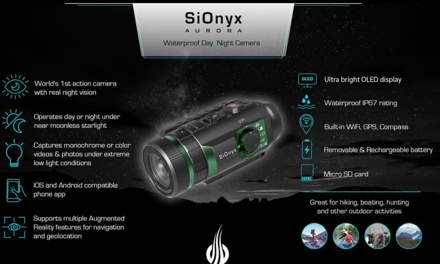
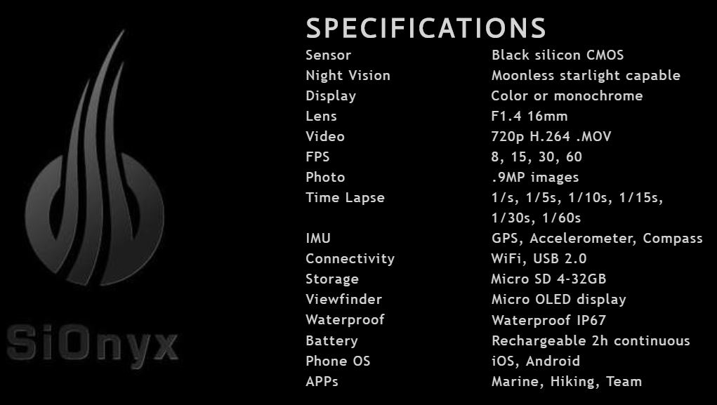
SiOnyx Announces Consumer Black Silicon Camera
SiOnyx presents Aurora action camera based on Black Silicon image sensor that it will be launching on Kickstarter on April 20th:


SWIR Vision Systems Startup
PRNewswire: RTI International, a nonprofit research institute, spins-out a venture company, SWIR Vision Systems Inc., to commercialize infrared camera technology developed at RTI for applications in the industrial machine vision, security systems, agricultural, automotive, and other global imaging markets.
RTI's patented infrared camera technology, based on novel and commercially scalable image sensor materials, was advanced with a combination of grant support from DARPA and internal development, management, and financial support from RTI. The technology was licensed exclusively to SWIR Vision Systems, which plans to commercialize its SWIR-band cameras in 2018 and manufacture the cameras at its Research Triangle Park, NC operations center.
George Wildeman, a photonics industry executive and entrepreneur with over 25 years of technology commercialization experience, has been named CEO of SWIR Vision Systems. Ethan Klem will transition from RTI to become SWIR's CTO.
"Acuros cameras will dramatically expand the imaging toolkit for machine vision integrators, disrupting the cost and performance curve for vision systems design," said Wildeman, "We look forward to witnessing the impact of the technology as it is adopted in our target applications and markets."
The challenge: Expensive InGaAs Sensors
Presently, commercially available, short-wave infrared (SWIR) imagers are based on costly, high-purity semiconductor materials such as indium-gallium-arsenide (InGaAs) that are grown on indium phosphide (InP) substrate. To form electrical connections between each photodiode (i.e., pixel) and the corresponding Si ROIC input, the two devices are joined, one detector at a time, by metal-to-metal bonding. This time-consuming process, known as hybridization, is carried out by forming an array of bumps on the detector die, bringing this bumped array into contact with an array of metal bumps on the ROIC die, and then reflowing the bonds to form the electrical connections. The hybridization process imposes limitations on array size, pixel size, and sensor resolution.
The innovation: CQD Sensor Technology
CQD sensor technology changes the performance-to-cost point of SWIR cameras. CQD semiconductor crystals are deposited from solution directly on the surface of silicon CMOS circuitry. The resulting monolithic photodetector structure enables higher resolution and eliminates the prohibitively expensive hybridization process inherent to InGaAs sensors.


Tuesday, March 27, 2018
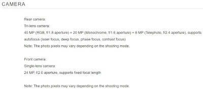
Huawei Unveils Smartphone with Triple 40MP Rear Camera
BusinessWire: Huawei P20 Pro flagship smartphone features triple rear camera and DxOMark Photo score of 114 points:
"The HUAWEI P20 Pro features a Leica triple camera with the highest total pixel count on a smartphone – the camera configuration is comprised of a 40MP RGB sensor, a 20MP monochrome sensor and an 8MP sensor with telephoto lens. It also features an exclusive Leica color temperature sensor for better color reproduction. With f/1.8, f/1.6 and f/2.4 wide aperture to capture crisp, clear details, the HUAWEI P20 Pro also includes a brand new Leica 3x telephoto (VARIO-SUMMILUX-H 1:1.6-2.4/27-80ASPH) lens for long-range photography of up to 5x Hybrid Zoom. The HUAWEI P20 Pro’s highly sensitive image sensor captures low light photos with up to ISO 102400.
The HUAWEI P20 builds on its predecessor’s foundation with a Leica dual camera featuring a 12MP sensor with a pixel size as high as 1.55 μm, and a 20MP monochrome sensor, enhancing the HUAWEI P20’s ability to capture photos in low-light settings.
The HUAWEI P20 Series devices support six-axis stabilization and 960fps super slow motion. With Ultra Snapshot mode, the devices can capture an image in as little as 0.3 seconds by just double clicking the down volume button, even from an off screen."
Key camera data:
- Triple camera setup
- Main camera: 40Mp, 1/1.73″ RGB sensor with Quad Bayer structure, f/1.8-aperture lens with 27mm equivalent focal length
- Secondary camera: 20Mp, 1/2.78″ monochrome sensor, f/1.6-aperture lens with 27mm equivalent focal length
- Tele-camera: 8Mp, 1/4.4″ RGB sensor, f/2.4-aperture lens with 80mm equivalent focal length, and optical image stabilization
- Aperture mode default eq. focal length: 55mm
- PDAF on main sensor
- 4K video (not default mode)
- 960 fps slow-motion video at 720p


Monday, March 26, 2018
Caeleste Updates on its Low Noise Pixels
Caeleste updates on the recent progress in its low noise pixels based on the combination of oversampling and inversion-accumulation cycling:
"Pixel with thin gate oxide narrow pmos amplifier has the lowest noise. Because of process variation, even the same kind of pixels has some noise difference. For pixels with thin gate oxide narrow pmos amplifier, the best pixel can reach 0.21 e-RMS read noise."

"Pixel with thin gate oxide narrow pmos amplifier has the lowest noise. Because of process variation, even the same kind of pixels has some noise difference. For pixels with thin gate oxide narrow pmos amplifier, the best pixel can reach 0.21 e-RMS read noise."
Passive IR Sensors Tutorial
EE Journal publishes a tutorial video on passive IR sensors by Amelia Dalton and Jeffrey Katz (Panasonic):
Sunday, March 25, 2018
Sony Discloses PDAF Usable up to the Array Edges
Sony patent application US20180077372 "Solid-state imaging element and driving method therefor, and electronic apparatus" by Hiroaki Ishiwata proposes keeping the TG shape constant even though the PDAF diodes ratio changes across the array.
In interchangeable lens cameras, "if lenses having different F-values are used, there is a possibility that the light-collecting spot S may be deviated from the center of the pixel. In this case, in order to set the light-collecting spot S in the boundary between the phase-difference pixel A and the phase-difference pixel B, it is necessary to set the light-receiving surfaces of the phase-difference pixel A and the phase-difference pixel B to have a different size. The light-collecting spot position is changed depending on an image height, and hence it is necessary to change, depending on the arrangement position of the pixels in the solid-state imaging element, the size ratio between the phase-difference pixels A and B in that pixel."


In interchangeable lens cameras, "if lenses having different F-values are used, there is a possibility that the light-collecting spot S may be deviated from the center of the pixel. In this case, in order to set the light-collecting spot S in the boundary between the phase-difference pixel A and the phase-difference pixel B, it is necessary to set the light-receiving surfaces of the phase-difference pixel A and the phase-difference pixel B to have a different size. The light-collecting spot position is changed depending on an image height, and hence it is necessary to change, depending on the arrangement position of the pixels in the solid-state imaging element, the size ratio between the phase-difference pixels A and B in that pixel."


ON Semi Proposes Image Sensor With Improved PSRR
OM Semi patent application US20180077368 "Image sensors with power supply noise rejection capabilities" by Kazuhisa Suzuki explains the mechanisms of supply noise influence and proposes an improvement:


2018 Image Sensors Europe Awards
Image Sensors Europe conference held in London, UK in mid-March publishes its 2018 Awards:
Best Academic Research Team
Winner: Robert Henderson and his team at The University of Edinburgh
Best Up-and-Coming Company
Winner: vivaMOS Ltd
"The challenges faced for the design of wafer-scale image sensors required a rethinking of the traditional methods used and developed for semiconductor ASIC design. Good pixel design know-how with expertise in analogue mixed-signal and radiation-hard designs is the foundation on which the sensors are developed for good imaging performance in harsh X-ray environments. However, developing products of such a significant size has required a new thought-process and approach. We are delighted to have been recognised with another industry award. The recognition from industry peers is testimony to the hard work and ingenuity that the vivaMOS team has put into this new business." - Dan Cathie, CEO
Biggest Breakthrough Development
Winner: ams AG for CMV50000 image sensor.
Biggest Innovator in the Image Sensor Industry
Winner: Xenics NV
"We thank the judges for recognizing the breakthrough achieved by the development of our latest XLIN detector, and also to our engineers who made it all possible."
CEO/Managing Director of the Year
Winner: Omer Keilaf, CEO and Co-founder, Innoviz Technologies

Saturday, March 24, 2018
LiDARs at Image Sensors Europe 2018
Imaging and Machine Vision Europe publishes a review of LiDAR presentations at Image Sensors Europe conference held in mid-March in London, UK. Few quotes:
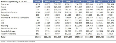
"A report from Goldman Sachs Global Investment Research predicts that the market opportunity for lidar in automotive will grow from zero in 2015 to $10 billion by 2025, and $35 billion by 2030.
Oren Rosenzweig, co-founder of Israeli lidar system maker Innoviz Technologies, said at Image Sensors that the cost of lidar is prohibitive, and the performance is not good enough. Rosenzweig, speaking to Imaging and Machine Vision Europe at the show, said that $1,000 per lidar system might be acceptable for certain early adopters of the technology, but that hundreds of dollars per lidar was needed to make it attractive to automotive OEMs. As the volumes increase, however, then costs will go down.
Innoviz’s technology is a solid-state lidar combining a MEMS scanner based on a micro-mirror designed by the company; the signal is processed in a proprietary ASIC. The Innoviz One has a 250-metre detection range, an angular resolution of 0.1 x 0.1 degrees, a frame rate of 25fps, and a depth accuracy of 3cm. The device is based on 905nm laser light; 1,550nm would cost too much for the lasers and detectors, Rosenzweig said.
Solid-state lidar uses primarily 905nm lasers, according to Carl Jackson, founder and CTO of SensL, although he added that 940nm VCSEL arrays are also being developed. Jackson said that SiPMs or a SiPM array can improve sensitivity and ranging compared to avalanche photodiodes (APDs).
SensL’s first product for lidar is a 400 x 100 ToF SPAD array with high dynamic range SPAD pixels, optimised for vertical line scanning. It will be sampling in the second half of 2018. Jackson said that the sensor array can be used to create a lidar solution with 0.1 degree x-y resolution, suitable for greater than 100-metre ranging at 10 per cent reflectivity in full sunlight. Jackson also noted that VGA-quality SPAD arrays could be available next year.
Eye-safety is all about the design of the system, according to Jackson. He said that a laser pulse of 1ns from a 5mm aperture at 30 degrees angle of view in the y direction can reach 26,908W of power and still be eye safe, ‘which is plenty of power to do long-range lidar with 905nm’. He added that a 120 x 30-degree system will need 6,000W of laser power to achieve 200-metre ranging with SiPM technology."
"A report from Goldman Sachs Global Investment Research predicts that the market opportunity for lidar in automotive will grow from zero in 2015 to $10 billion by 2025, and $35 billion by 2030.

Oren Rosenzweig, co-founder of Israeli lidar system maker Innoviz Technologies, said at Image Sensors that the cost of lidar is prohibitive, and the performance is not good enough. Rosenzweig, speaking to Imaging and Machine Vision Europe at the show, said that $1,000 per lidar system might be acceptable for certain early adopters of the technology, but that hundreds of dollars per lidar was needed to make it attractive to automotive OEMs. As the volumes increase, however, then costs will go down.
Innoviz’s technology is a solid-state lidar combining a MEMS scanner based on a micro-mirror designed by the company; the signal is processed in a proprietary ASIC. The Innoviz One has a 250-metre detection range, an angular resolution of 0.1 x 0.1 degrees, a frame rate of 25fps, and a depth accuracy of 3cm. The device is based on 905nm laser light; 1,550nm would cost too much for the lasers and detectors, Rosenzweig said.
Solid-state lidar uses primarily 905nm lasers, according to Carl Jackson, founder and CTO of SensL, although he added that 940nm VCSEL arrays are also being developed. Jackson said that SiPMs or a SiPM array can improve sensitivity and ranging compared to avalanche photodiodes (APDs).
SensL’s first product for lidar is a 400 x 100 ToF SPAD array with high dynamic range SPAD pixels, optimised for vertical line scanning. It will be sampling in the second half of 2018. Jackson said that the sensor array can be used to create a lidar solution with 0.1 degree x-y resolution, suitable for greater than 100-metre ranging at 10 per cent reflectivity in full sunlight. Jackson also noted that VGA-quality SPAD arrays could be available next year.
Eye-safety is all about the design of the system, according to Jackson. He said that a laser pulse of 1ns from a 5mm aperture at 30 degrees angle of view in the y direction can reach 26,908W of power and still be eye safe, ‘which is plenty of power to do long-range lidar with 905nm’. He added that a 120 x 30-degree system will need 6,000W of laser power to achieve 200-metre ranging with SiPM technology."
Thursday, March 22, 2018
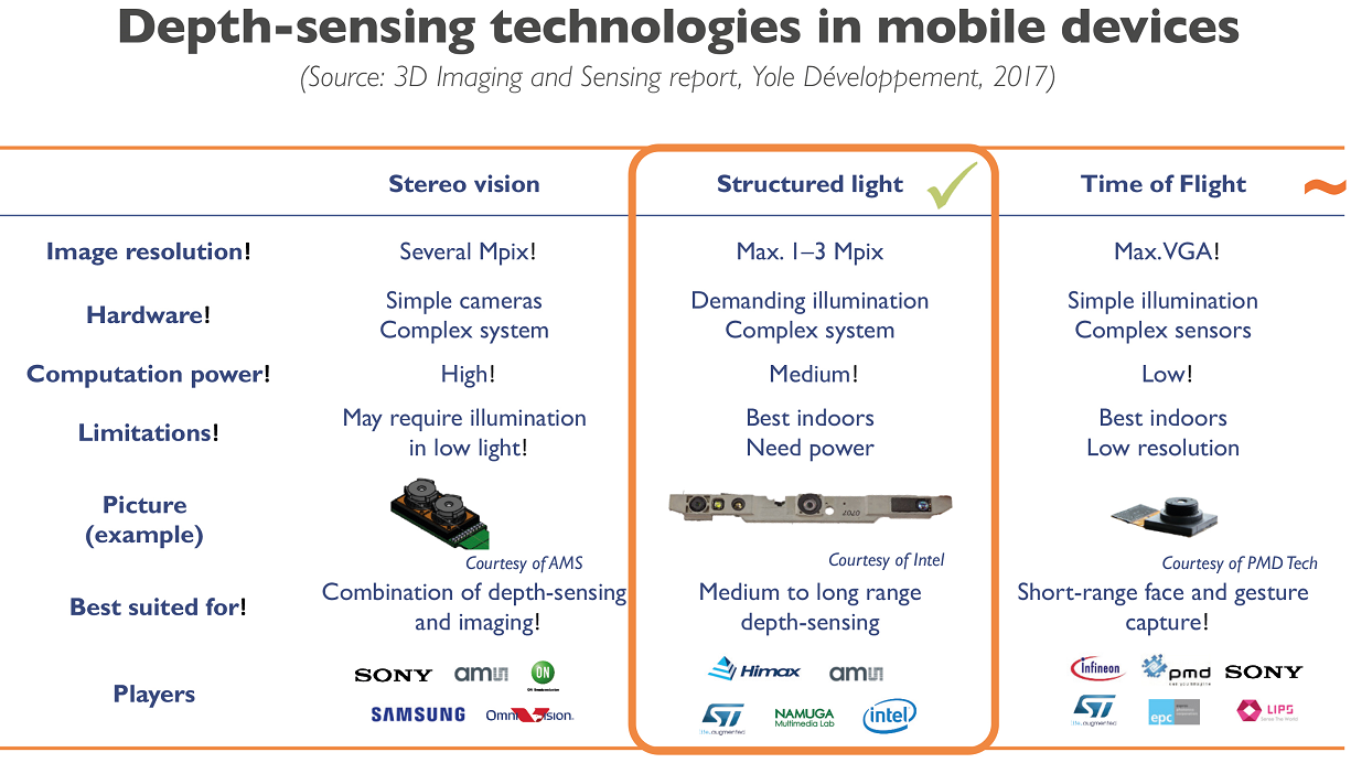
Smartphone Companies Scrambling to Match Apple 3D Camera Performance and Cost
EETimes publishes an article "Can Huawei Match Apple TrueDepth?" by Junko Yoshida. Few quotes:
Pierre Cambou, activity leader for MEMS and imaging at Yole Développement, predicts that it may take a year or longer for competitors to offer 3D sensing technologies comparable to iPhone X.
...3D sensing will be a tougher challenge for most smartphone vendors — because a 3D camera contains myriad components that need to be aligned. It also requires competent supply chain management. Cambou called the 3D camera “a bundle of sub-devices.”
As for Samsung’s Galaxy S9, some reviewers are already calling its front-facing sensing technology “a disappointment.” ...People were able to fool Samsung's technology on last year's Galaxy S8 by using photos. Apparently, that trick still works with the S9.
Huawei’s triple cameras appear to illustrate the company’s effort to enhance depth-sensing technology. While no confirmation is available, Huawei’s suspected 3D sensing partner is Qualcomm.

Reuters shares the same opinion:
Most Android phones will have to wait until 2019 to duplicate the 3D sensing feature behind Apple’s Face ID security, three major parts producers have told Reuters.
According to parts manufacturers Viavi Solutions Inc, Finisar Corp and Ams AG, bottlenecks on key parts will mean mass adoption of 3D sensing will not happen until next year, disappointing earlier expectations.
Tech research house Gartner predicts that by 2021, 40 percent of smartphones will be equipped with 3D cameras, which can also be used for so-called augmented reality.
Pierre Cambou, activity leader for MEMS and imaging at Yole Développement, predicts that it may take a year or longer for competitors to offer 3D sensing technologies comparable to iPhone X.
...3D sensing will be a tougher challenge for most smartphone vendors — because a 3D camera contains myriad components that need to be aligned. It also requires competent supply chain management. Cambou called the 3D camera “a bundle of sub-devices.”
As for Samsung’s Galaxy S9, some reviewers are already calling its front-facing sensing technology “a disappointment.” ...People were able to fool Samsung's technology on last year's Galaxy S8 by using photos. Apparently, that trick still works with the S9.
Huawei’s triple cameras appear to illustrate the company’s effort to enhance depth-sensing technology. While no confirmation is available, Huawei’s suspected 3D sensing partner is Qualcomm.
 |
| SystemPlus' and Yole's cost estimation of iPhone X 3D camera |

Reuters shares the same opinion:
Most Android phones will have to wait until 2019 to duplicate the 3D sensing feature behind Apple’s Face ID security, three major parts producers have told Reuters.
According to parts manufacturers Viavi Solutions Inc, Finisar Corp and Ams AG, bottlenecks on key parts will mean mass adoption of 3D sensing will not happen until next year, disappointing earlier expectations.
Tech research house Gartner predicts that by 2021, 40 percent of smartphones will be equipped with 3D cameras, which can also be used for so-called augmented reality.
Blackmore Raises $18M for Coherent LiDAR
PRNewswire: Bozeman, Montana-based Blackmore Sensors and Analytics Inc. has raised $18m in a Series B funding led by BMW i Ventures. Additional investment comes from Toyota AI Ventures, Millennium Technology Value Partners and Next Frontier Capital.
"Blackmore has unique and innovative FMCW lidar technology that delivers a new dimension of data to future vehicles," said BMW i Ventures partner Zach Barasz. In addition to being more cost-effective, Blackmore's FMCW lidar has several advantages over traditional pulsed lidar systems.
"Blackmore's groundbreaking FMCW lidar technology is designed to eliminate interference, improve long-range performance, and support both range and velocity — a triple threat to make autonomous driving safer," said Jim Adler, managing director of Toyota AI Ventures.
According to Randy Reibel, Blackmore's CEO, it is that last capability that differentiates Blackmore's sensor from its competitors. "Having the ability to measure both the speed and the distance to any object gives self-driving systems more information to navigate safely."
Blackmore will use the investment to scale the production of its FMCW lidar for ADAS and self-driving markets. Increased production capacity will allow Blackmore to support the growing sector of autonomous driving teams demanding a superior lidar solution.


Wednesday, March 21, 2018
ToF Depth Resolution Improved to 6.5nm
OSA Optics Letters issue dated by April 1st, 2018 publishes Peking University, China, KAIST and KRISS, Korea paper "Time-of-flight detection of femtosecond laser pulses for precise measurement of large microelectronic step height."
"By using time-of-flight detection with fiber-loop optical-microwave phase detectors, precise measurement of large step height is realized. The proposed method shows uncertainties of 15 nm and 6.5 nm at sampling periods of 40 ms and 800 ms, respectively. This method employs only one free-running femtosecond mode-locked laser and requires no scanning of laser repetition rate, making it easier to operate. Precise measurements of 6 μm and 0.5 mm step heights have been demonstrated, which show good functionality of this method for measurement of step heights."
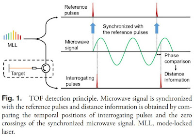

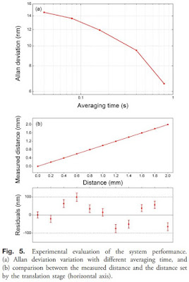
"By using time-of-flight detection with fiber-loop optical-microwave phase detectors, precise measurement of large step height is realized. The proposed method shows uncertainties of 15 nm and 6.5 nm at sampling periods of 40 ms and 800 ms, respectively. This method employs only one free-running femtosecond mode-locked laser and requires no scanning of laser repetition rate, making it easier to operate. Precise measurements of 6 μm and 0.5 mm step heights have been demonstrated, which show good functionality of this method for measurement of step heights."


Subscribe to:
Posts (Atom)